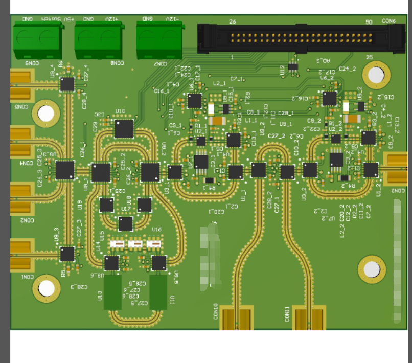
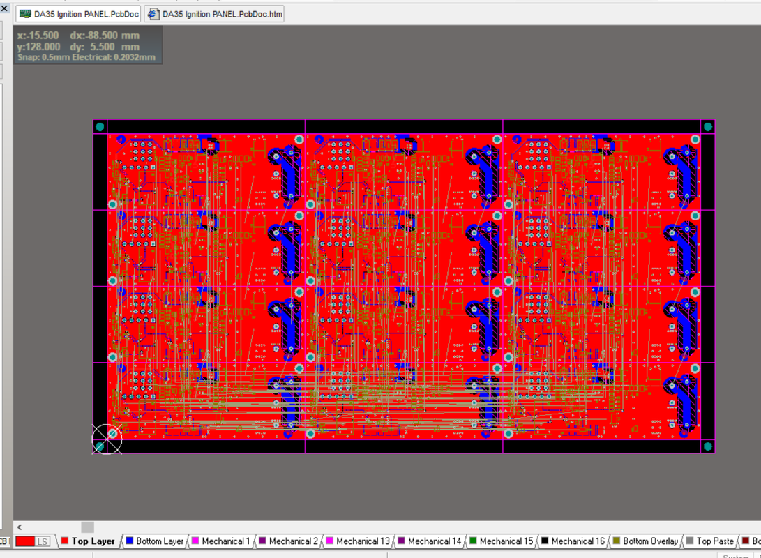
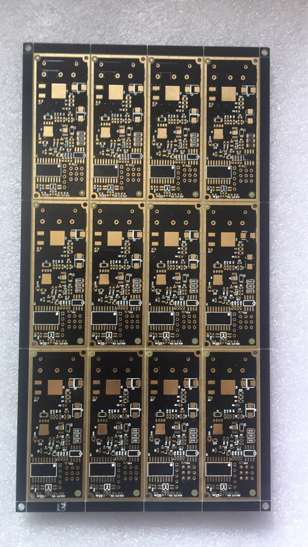
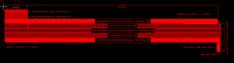
Because of bad experience with weebly.We can not enable SSL for many years,but weebly can not fix this issue.Our latest news change to this link
https://www.stormpcb.com/PCBnews
How we make assembly boards from your Altium or gerber file ? Below is a simple process.
1, We will export gerber file from your Altium .(Gerber file is preferred to us ) 2,We will quote with your BOM and PCB file. any of your products photos will be helpful and 3D file. 3,PCB manufacturing following gerber. there are over 30 processes to do .drill -->plate. see our PCB process.WorkShop 4,In the meanwhile of PCB manufacturing,we will purchase components with your approved BOM. 5,PCB assembly,including SMT loading and Through hole soldering. 6,Final inspecting and photos to approve.
0 Comments
We know most of Al-substrate are single sided boards,but ,yes,there are always some exceptions. Some Al-substrate boards need to be doubles sided.We made a few of such boards,but designer always do not know what they want or what they designed.They do not know the Al-substrate is in the middle or at the bottom side . Unlike FR4 PCB,any core-substrate boards have two types.One is sandwitch type as the Al-substrate is at the middle of board,like a sandwitch.Another is blind type. See above for the Al-substrate boards stackup.All of metal-substrate boards like this too.Many double-sided metal-substrate boards used the first type--sandwitch .The metail is at the middle of the board.
Sandwtich Al board process is Al-susbtrate cutting --->drilling-->anodic oxidation--->stackup-->drilling, the last is the same as usual FR4 double layer board process. Another type--blind type ,process is Al-susbtrate cutting --->drilling-->anodic oxidation FR4 cutting --->drilling--->plating--->L2 layer---->stackup with above --->L1 layer--> the last is the same as FR4 double sided board process. From the stackup,the hole is the main difference.The holes are through from TOP to Bottom side on sanswtch type.we can see holes easily. Blind type,the holes are not through,the bottom side is the Alminum. So,when you design a double sided Al-substrate board,you can indicate it is Sandwitch or blind type or send us the stackup you want . Chamfer,usually,we say "Chamfer" means golden fingers chamfer.The gold fingers are in the same straight line,there is no problem to do such chamfers. like below. Our robot customer has a new design ,the Printed Circuit board in the design is round and it has a special shape to fit in the robot case. The chamfer is a circle and we must do it in the slots.
Components quality is the key important for any electronics devices. We also had a lot of problems for the components purchased from non-Authorized Distributors before.In 2017, we had two projects rejected with the bad electronic components. MAX485ECSA is the big problem,it made us and our customer on a fire position. There are many many fake/used parts,MAX part is just one of them. In 2019,we have improved our purchasing process, for the key components--chip,MCU or any other components which you required,we will buy from authorized distributors,eg,digikey,mouser,etc. Here are some components we purchased from Mouser directly.Do not worry about our components quality now.We will follow your part number and get the original&new parts to assemble.
Our great country--The People's Republic of China has celebrated 70 years of Communist party rule and its rise to global superpower status with a military parade showcasing the country’s technology, and a promise from President Xi Jinping that “no force can shake the status of this great nation”. Wish our great motherland prosperity and prosperity. Flexible circuit boards made by Storm Circuit.
Fine pitch 0.075mm/0.075mm (3/3mil) FR4 1.2mm stiffener + PI 2mil stiffener 2 layer FPC Stackup: Shengyi SF302C 0.5oz copper Shengyi SF302 0.5oz copper Shengyi SF302C How to prove ENEPIG is used in your PCB? Spectrum can say anything. One of our American college clients provided us what they saw in the PCB pads with a spectrometer.We made a lot of ENEPIG (Electroless Nickel Electroless Palladium Immersion Gold) circuit boards for all of our customers in the world.You may would like to know more about ENEPIG,please click here. Spectrum confirms the presence of Nickel (Ni), Gold (Au), and Palladium (Pd). ENEPIG is capable of meeting more stringent requirements of multiple types of packages including THT (through-hole technology), SMT, BGA, wire bonding, press fit etc. What's better, ENEPIG is also suitable for PCBs with different packaging technologies. As a result, application fields ENEPIG can serve include aerospace, military ,Telecommunication equipments and high performance devices and medical industries with higher requirement of density and reliability.
Smart devices are smaller and smaller ,but smarter. This has promoted the continuous progress of PCB technology,any layer HDI,laser drilling,back drilling ,etc. We must embrace new technologies and growing with it. Below is an example what we did.it is a 4 layer board with 1.0mm,but the blind via is from L1-L2. The blind via is only 0.075mm in the BGA pad. via in pad is must to do at the BGA area. PCB specification: FR4,1.0mm,4 layer. min hole 0.075mm, laser driling blind via ,via in pad technology. gap between hole edge to trace is only 0.128mm. You may say,oh ,it is not a very difficult printed circuit. But,actually,the key technology is the gap between the hole edge to the trace is only 0.13mm (5mil).Usually,the gap should be more than 0.2mm,but there is no space and the trace is only 0.076mm (3mil). hole is 0.075mm, laser drilling
|
sales@stormcircuit.com All rights reserved,2007-2020 Storm Circuit Technology Ltd
|
|