Storm Circuit Blog
  • Home
  • PCB Fab
    • Standard PCB
    • ENEPIG PCB
    • HDI PCB
    • Impedance Control
    • Heavy Copper PCB
    • Via in Pad
    • Quick Turn PCB
    • 10 layer PCB
    • High frequency PCB
    • MC/Aluminum PCB
    • Half hole plating
    • FPC Rigid-flex PCB
    • StormProto PCB
  • Technology
    • PCB Terminology
    • PCB Material
    • PCB Stackup
    • Blind and burrid vias
    • Tip for PCB design
    • Generate gerber from Altium
    • Design guide for Flexible PCB
  • Blog
  • Product

Tips for PCB design From PCB manufacturing side

  1. File format  ---Gerber with 274-x is preferred to manufaturing. If you send us with original design  file ,please send PDFs to see how the board looks like. Do not forget drill file in zip to us.We can read Altium, Protel , Eagle. KiCAD, PowerPCB, ODB++.
  2. The best PCB dimension to do and assemble is under 200*300mm,max 450*450mm for normal boards. if under 25.4*25.4mm,please panelise or contact us free to panelize for you .
  3. Add at least 5mm frames at two sides ,10mm at each sides is the best when loading.
  4.  Some customers need mouse bits (tab) to connect boards,not v-groove. The stamp holes should   be in 0.5-0.8mm.Contact us to get details for tab connecting.
  5.  Impedence control board,please inform us width/space ,layer,and what value you want.see an  example.
  6. Heavy copper PCB,you need to enlarge copper width and space.
  7. The standard stack up for multilayer board. Download here
  8. The check list for PCB manufacturing.Download here.
  9. How to generate gerber and drill files from Altium? pls see click.
  10. How to design Flexible circuits or Rigid-flex PCB? Here is a A guide book for designers of flexible circuits and Rigid-flex.
Do not forget the layer order to PCB manufacturer.it is Top/G1/GP1/Bottom or Top/GP1/G1/Bottom. You can define the layer order in gerber or drawing file.
CAM Engineering
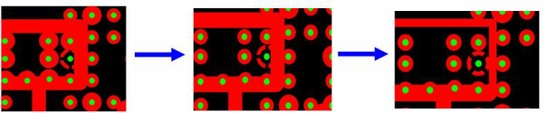
Our MI and CAM engineers have 5+ years experience.the left side is an example that many customers designed inner layer short or open circuit.
We have the eagle eye to pick this out and optimize the designs to perfect manufacturing process.

Open Circuit Design                  Not Good Design                     Perfect Design

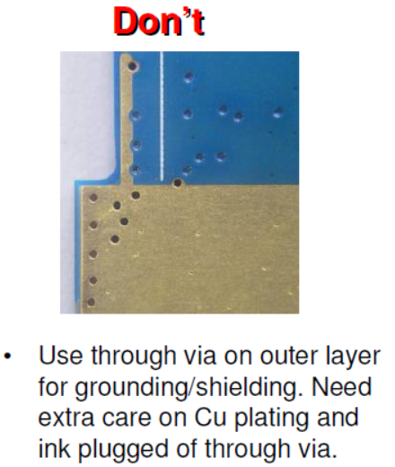
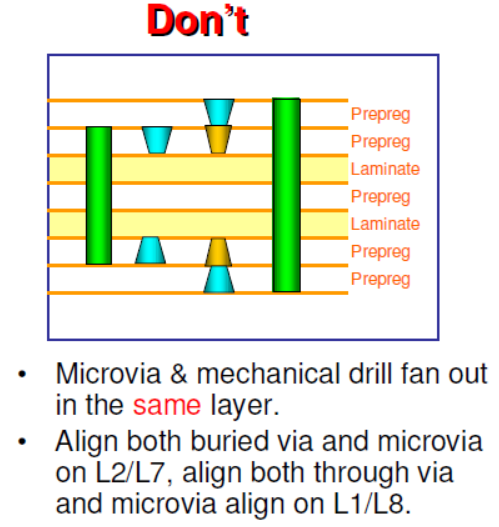
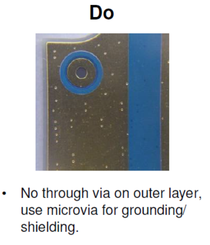
HDI holes design tips

Picture
Picture
Picture
Picture

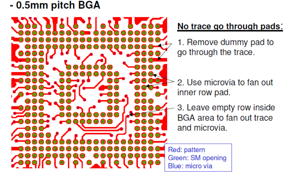
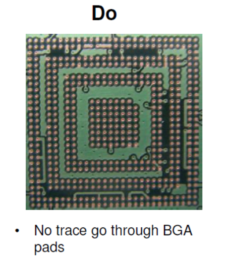
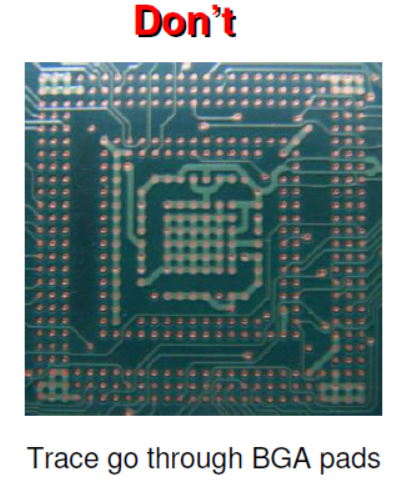
0.5mm pitch BGA design tips

0.5mm pitch BGA
Picture
Picture

0.4mm pitch BGA design tips

Picture
Questions? Please email us now.
Picture
About Us
Why Us
WorkShop
Quality
Testimonials
​Contact Us
Technology
Any layer HDI  PCB
Generate Gerber
Rigid-Flex Design Guide
10 Layer PCB
Impedance control
Heavy Copper PCB
​PCB Assembly
Quick Turn Circuits
HDI boards
Rigid-Flex circuits
RF/Microwave/HF PCB
MC PCB/Al-substrate
ENEPIG PCB
​Components procument


Payment
Shipment
FAQ
StormProto
SMT stencil
Via in Pad


Download
PCB Capability
Sample BOM
PCB check list
Multilayer stack up
​Stencils
PCB material

​
sales@stormcircuit.com​​             All rights reserved,2007-2020 Storm Circuit Technology Ltd
Picture
www.stormpcb.com
www.stormcircuit.com
Picture
Picture
Made with love by Storm Circuit in China

Picture
Picture
Picture

    news and discount

Subscribe
  • Home
  • PCB Fab
    • Standard PCB
    • ENEPIG PCB
    • HDI PCB
    • Impedance Control
    • Heavy Copper PCB
    • Via in Pad
    • Quick Turn PCB
    • 10 layer PCB
    • High frequency PCB
    • MC/Aluminum PCB
    • Half hole plating
    • FPC Rigid-flex PCB
    • StormProto PCB
  • Technology
    • PCB Terminology
    • PCB Material
    • PCB Stackup
    • Blind and burrid vias
    • Tip for PCB design
    • Generate gerber from Altium
    • Design guide for Flexible PCB
  • Blog
  • Product