HDI-HIGH DENSITY INTERCONNECT PCB
HDI PCBs capitalize on the latest technologies available to increase the functionality of PCBs using the same or less amount of area. This advancement in PCB technology is driven by the miniaturization of components and semiconductor packages that supports advanced features in revolutionary new products such as touch screen computing and 4G network communications.
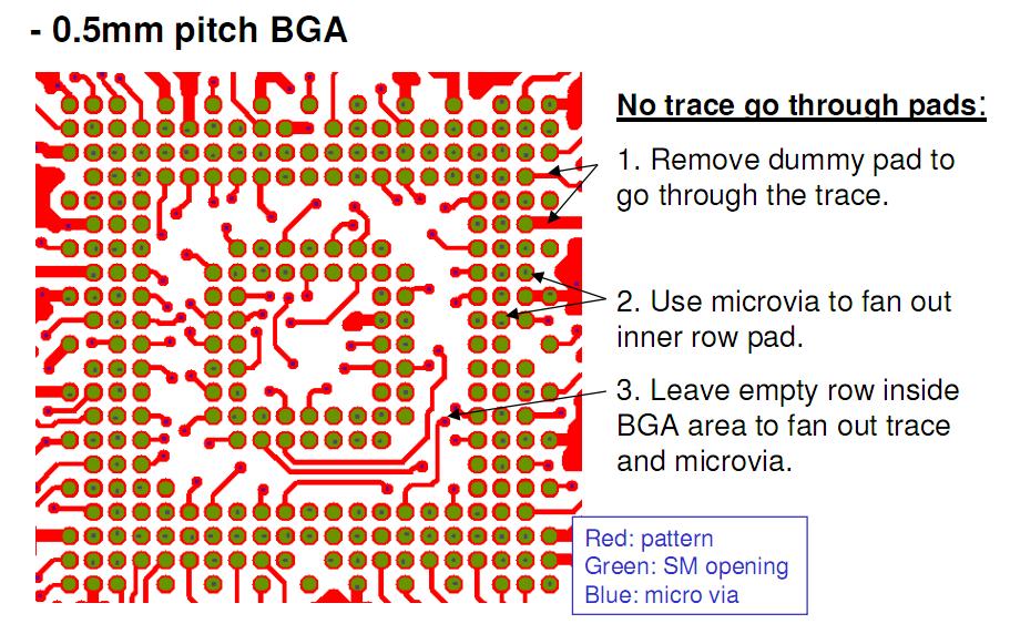
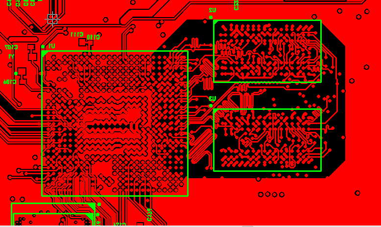
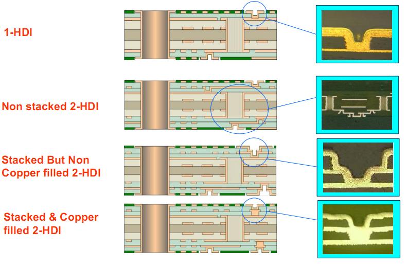
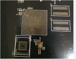
HDI PCBs are characterized by high-density attributes including laser microvias, fine lines and high performance thin materials. This increased density enables more functions per unit area. Higher technology HDI PCBs have multiple layers of copper filled stacked microvias (Advanced HDI PCBs) which creates a structure that enables even more complex interconnections. These very complex structures provide the necessary routing solutions for today's large pin-count chips utilized in mobile devices and other high technology products. Most HDI boards are with burried/blind vias from 0.076-0..127mm. Vias for HDI is 3-5 mil (0.076-0.127mm),line width is from 3-4mil(0.076-0.1mm). 0.8mm /0.5mm pitch BGA is usually for 1+N+1. Another thing is many customers did not know HDI board have to use special material--RCC (Resion Coated Copper),0.08mm thickness with copper. HDI 1+N+1,standard and quick turn lead time for prototypes .(<1 sq meter)
|
Download
Multilayer standard stack up PCB Fab check list PCB capability Sample BOM Flex PCB material High frequency material 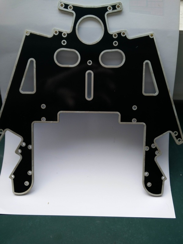
Immersion Silver ,2.4mm
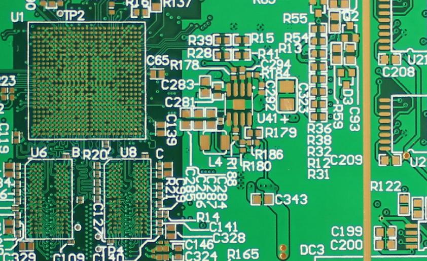
Our PCBs
Flex PCB Rigid-flex PCB RF board Heavy copper PCB 20 layer PCB 10 layer PCB HDI PCB ENEPIG PCB Control impedance Quick Turn boards MC PCB 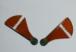
4 layer rigid-flex board
|

|
sales@stormcircuit.com All rights reserved,2007-2020 Storm Circuit Technology Ltd
|
|