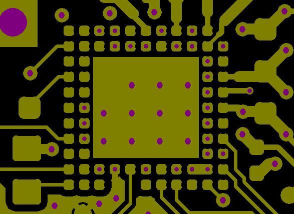
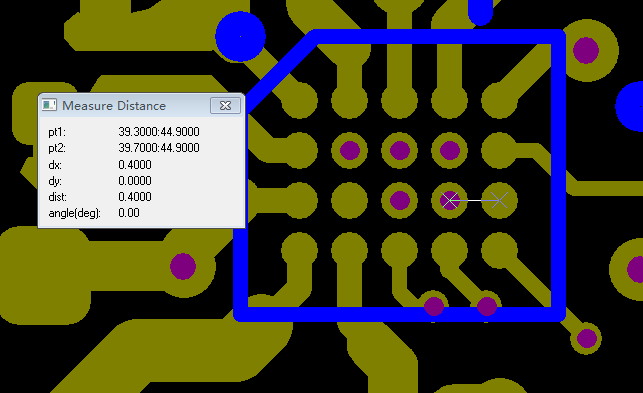
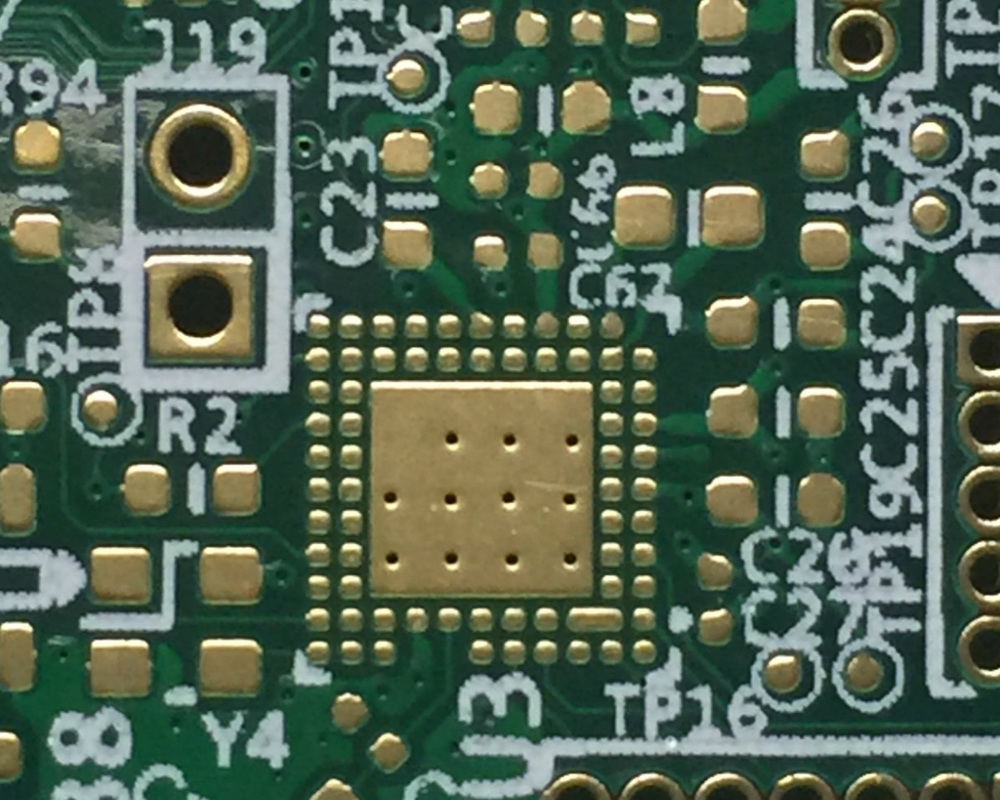
Storm Circuit Blog
  • Home
  • PCB Fab
    • Standard PCB
    • ENEPIG PCB
    • HDI PCB
    • Impedance Control
    • Heavy Copper PCB
    • Via in Pad
    • Quick Turn PCB
    • 10 layer PCB
    • High frequency PCB
    • MC/Aluminum PCB
    • Half hole plating
    • FPC Rigid-flex PCB
    • StormProto PCB
  • Technology
    • PCB Terminology
    • PCB Material
    • PCB Stackup
    • Blind and burrid vias
    • Tip for PCB design
    • Generate gerber from Altium
    • Design guide for Flexible PCB
  • Blog
  • Product

Via in Pad Technology

What is Via in Pad? In shortly,via in pad is the via holes are at the SMD pad.The vias are very small,usually under 0.3mm.Why and how? First is there is no enough space to layout,you have to put the vias and holes closer even together.Second it helps thermal management and for high frequency boards,it may help improve signals.
Because the SMD pads are for SMD components loading,so the solder can not flow to inner layer or the other side when assemble.That is the most important for via in pad board.
How PCB manufacturers like us to do via in pad board? We will fill all vias with non-conductive epoxy and plate copper over it ,so the vias are flat same as others. Many PCB factories are unable to do such capability.
The key technology is how we fill vias and guarantee there is no any solder (surface finishing) in the holes.
Filled via in pad is a way to achieve intermediate density with an intermediate cost compared to using blind/buried vias. Some of the key advantages associated with using the via in pad technology are:
  • Fan out fine pitch (less than .75mm) BGAs
  • Meets closely packed placement requirements
  • Better thermal management
  • Overcomes high speed design issues and constraints i.e. low inductance
  • No via plugging is required at component locations
  • Provides a flat, coplanar surface for component attachment
Via in big pads are not a big problem.but for BGA,that is technology.As BGA pads are very small,10mil or 12mil,and there is no enough space.Manufacturing is not easy as other boards.

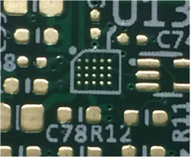
Here are some examples of what we did.

    Question? Contact Us Now.

    Your Name we contact you.
    We never spam.
    Your telephone we can contact you.
    Your Message to us.
    最大文件大小:20MB
    Please upload your Gerber file ,Altium,ODB++,CAM file.
Send
Via in pad in CAM file,BGA pad 10mil,via 0.15mm.
6 layer HDI board,0.1/0.1mm,
via in pad ,holes 0.15mm
via in pad ,BGA area,
0.4mm pitch BGA,via in pad
0.4mm pitch BGA ,via in pad
Real board,via in pad

via in pad,10 layer
via in pad,via is 0.15mm
0.4mm pitch BGA,via in pad
Real board with 0.4mm pitch BGA,via in pad
Download

Mullilayer standard stack up
PCB Fab check list 
PCB capability
Sample BOM
Flex PCB material
High frequency material
​stackup.pdfDesign guide for FPC
6 layer PCB with impedance control
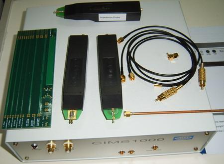
6 layer impedance control

Our PCBs

Flex PCB
Rigid-flex PCB
RF board
Heavy copper PCB
20 layer PCB
10 layer PCB
HDI PCB
ENEPIG PCB
Control impedance
Quick Turn boards
MC PCB
Via in Pad
BOSCH boards with peel mask
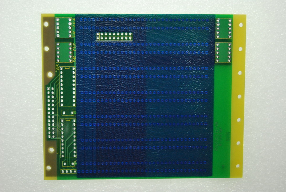
BOSCH boards with Peel mask
Additional Products&Service

Components Sourcing
PCB Assemble
SMT Stencil
Cable assemble

About Us
Why Us
WorkShop
Quality
Testimonials
​Contact Us
Technology
Any layer HDI  PCB
Generate Gerber
Rigid-Flex Design Guide
10 Layer PCB
Impedance control
Heavy Copper PCB
​PCB Assembly
Quick Turn Circuits
HDI boards
Rigid-Flex circuits
RF/Microwave/HF PCB
MC PCB/Al-substrate
ENEPIG PCB
​Components procument


Payment
Shipment
FAQ
StormProto
SMT stencil
Via in Pad


Download
PCB Capability
Sample BOM
PCB check list
Multilayer stack up
​Stencils
PCB material

​
sales@stormcircuit.com​​             All rights reserved,2007-2020 Storm Circuit Technology Ltd
Picture
www.stormpcb.com
www.stormcircuit.com
Picture
Picture
Made with love by Storm Circuit in China

Picture
Picture
Picture

    news and discount

Subscribe
  • Home
  • PCB Fab
    • Standard PCB
    • ENEPIG PCB
    • HDI PCB
    • Impedance Control
    • Heavy Copper PCB
    • Via in Pad
    • Quick Turn PCB
    • 10 layer PCB
    • High frequency PCB
    • MC/Aluminum PCB
    • Half hole plating
    • FPC Rigid-flex PCB
    • StormProto PCB
  • Technology
    • PCB Terminology
    • PCB Material
    • PCB Stackup
    • Blind and burrid vias
    • Tip for PCB design
    • Generate gerber from Altium
    • Design guide for Flexible PCB
  • Blog
  • Product