Storm Circuit Blog
  • Home
  • PCB Fab
    • Standard PCB
    • ENEPIG PCB
    • HDI PCB
    • Impedance Control
    • Heavy Copper PCB
    • Via in Pad
    • Quick Turn PCB
    • 10 layer PCB
    • High frequency PCB
    • MC/Aluminum PCB
    • Half hole plating
    • FPC Rigid-flex PCB
    • StormProto PCB
  • Technology
    • PCB Terminology
    • PCB Material
    • PCB Stackup
    • Blind and burrid vias
    • Tip for PCB design
    • Generate gerber from Altium
    • Design guide for Flexible PCB
  • Blog
  • Product

10 layer & 20 layer PCB

Usually,10 & 20 layers PCB are HDI board,but some are not .Some with big trace width and space,holes are over 0.3mm too. We have much experience in doing 10 layer PCB & 20 layer PCB.
A ten-layer board should be used when six routing layers are required.  Ten-layer boards, therefore, usually have six signal layers and four planes.  Having more than six signal layers on a ten-layer board is not recommended.  Ten-layers is also the largest number of layers that can usually be conveniently fabricated in a 0.062" thick board.  Occasionally you will see a twelve-layer board fabricated as a 0.062" thick board, but the number of fabricators capable of producing it are limited..

High layer count boards (ten +) require thin dielectrics (typically 0.006" or less on a 0.062" thick board) and therefore they automatically have tight coupling between layers.  When properly stacked and routed they can meet all of our objectives and will have excellent EMC performance and signal integrity.

A very common and nearly ideal stack-up for a ten-layer board is shown in Figure 12.  The reason that this stack-up has such good performance is the tight coupling of the signal and return planes, the shielding of the high-speed signal layers, the existence of multiple ground planes, as well as a tightly coupled power/ground plane pair in the center of the board.  High-speed signals normally would be routed on the signal layers buried between planes (layers 3-4 and 7-8 in this case).


Get PCB Quote Now
Examples of what we did for 10 and 20 layer PCBs.
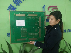
12 Layer high Tg PCB,5.0mm,564*502mm,countersink holes,pressfit holes +/-0.05mm,,used in test equipment
12 Layer high Tg PCB,5.0mm,564*502mm,countersink holes,pressfit holes +/-0.05mm
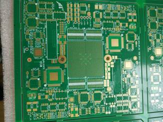
16 Layer PCB ,FR4, IT180,thickness 2.7mm,min trace/space 0.11/0.11mm, lead time 10 days.
16 Layer PCB ,FR4, IT180,thickness 2.7mm,min trace/space 0.11/0.11mm
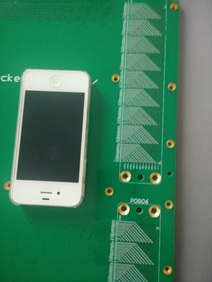
Countersink holes details,5 different holes in 12 layer board
Countersink holes details
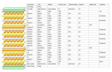
An example of 12 layer stack up
Download

Mullilayer standard stack upstackup.pdf
PCB Fab check list 
PCB capability
Sample BOM
Flex PCB material
High frequency material
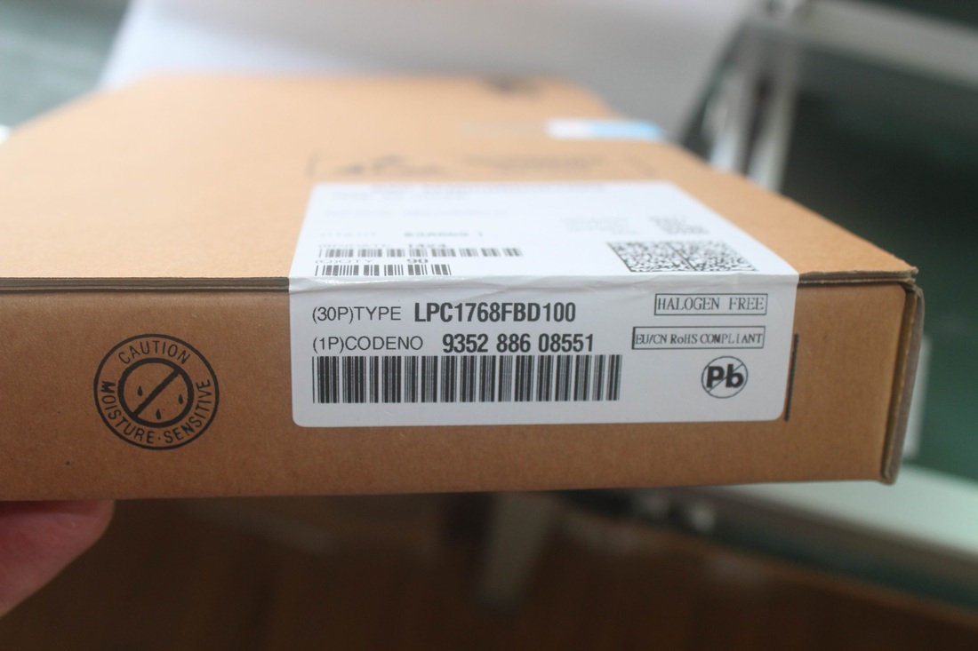
IC ,LPC178
Original&New LPC178 chips
Our PCBs

Flex PCB
Rigid-flex PCB
RF board
Heavy copper PCB
20 layer PCB
10 layer PCB
HDI PCB
ENEPIG PCB
Control impedance
Quick Turn boards
MC PCB
图片
Turnkey assembly service
Additional Products&Service
Components Sourcing
PCB Assemble
SMT Stencil
Cable assemble
About Us
Why Us
WorkShop
Quality
Testimonials
​Contact Us
Technology
Any layer HDI  PCB
Generate Gerber
Rigid-Flex Design Guide
10 Layer PCB
Impedance control
Heavy Copper PCB
​PCB Assembly
Quick Turn Circuits
HDI boards
Rigid-Flex circuits
RF/Microwave/HF PCB
MC PCB/Al-substrate
ENEPIG PCB
​Components procument


Payment
Shipment
FAQ
StormProto
SMT stencil
Via in Pad


Download
PCB Capability
Sample BOM
PCB check list
Multilayer stack up
​Stencils
PCB material

​
sales@stormcircuit.com​​             All rights reserved,2007-2020 Storm Circuit Technology Ltd
Picture
www.stormpcb.com
www.stormcircuit.com
Picture
Picture
Made with love by Storm Circuit in China

Picture
Picture
Picture

    news and discount

Subscribe
  • Home
  • PCB Fab
    • Standard PCB
    • ENEPIG PCB
    • HDI PCB
    • Impedance Control
    • Heavy Copper PCB
    • Via in Pad
    • Quick Turn PCB
    • 10 layer PCB
    • High frequency PCB
    • MC/Aluminum PCB
    • Half hole plating
    • FPC Rigid-flex PCB
    • StormProto PCB
  • Technology
    • PCB Terminology
    • PCB Material
    • PCB Stackup
    • Blind and burrid vias
    • Tip for PCB design
    • Generate gerber from Altium
    • Design guide for Flexible PCB
  • Blog
  • Product