Storm Circuit Blog
  • Home
  • PCB Fab
    • Standard PCB
    • ENEPIG PCB
    • HDI PCB
    • Impedance Control
    • Heavy Copper PCB
    • Via in Pad
    • Quick Turn PCB
    • 10 layer PCB
    • High frequency PCB
    • MC/Aluminum PCB
    • Half hole plating
    • FPC Rigid-flex PCB
    • StormProto PCB
  • Technology
    • PCB Terminology
    • PCB Material
    • PCB Stackup
    • Blind and burrid vias
    • Tip for PCB design
    • Generate gerber from Altium
    • Design guide for Flexible PCB
  • Blog
  • Product

Impedance Control PCB

Many customers asked us what information we need for impedence control PCB.Here,there are two types for PCB manufacturer,a is single impedance ,just one trace ,two holes .and b is differential impedance,it always go with 1 pair (two trace with same width and space). For single impedance,you just tell us the trace width one which layer and what value you require .For differential impedance,trace width/space,layers and value. Our experience engineers will calculate following your instruction with Polar software.We may change trace width/space or stackup ,but please do not worry, if any changes,we will send you to approve before proceeding. Generally,the tolerance is 10%,and more accurate is 8% .All impedance boards ,we will test here and report.

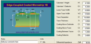
Here is an example of what information we need to do impedance control.
TYPE VALUE Layer width/space
Single 50 ohm +/-10% L1,L6 0.15mm
Single 50 ohm +/-10% L2,L3,L4,L5 0.13mm
Differential 90 ohm +/-10% L1,L6 0.13/0.13mm
Differential 100 ohm +/-10% L1,l6 0.13mm/0.2mm
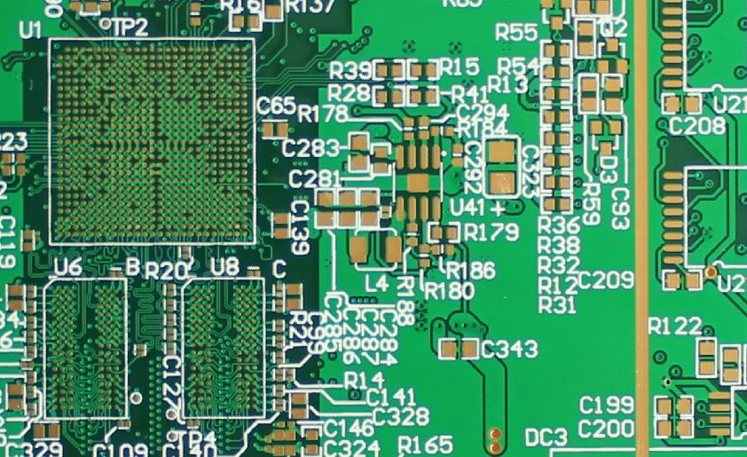
As a PCB manufacturer,we made a lot of impedance PCBs.Here are some of our suggestions for impedance calculation.The most important is the Er,H,W and T. Er is material dielectric constant.H is the dielectric thickness.W is trace width.​and T is trace thickness.The following are the calcluation models and stackups we often use.
Request Your Impedance Control PCB Now.
10 Layer HDI board,0.5mm pitch BGA. 4/4mil,0.15mm vias,Tablet PC mother board,Impedance control
10 layer HDI impedance control board
8 layer HDI board ,impedance control,4/4mil 0.15mm vias,Telecom board
8 laye HDI impedance control boards
An example of 6 layer impedance control coupon 
Picture
How we calculate the impedance value with our software before proceeding.
8 layer impedance coupon design
Download

Mullilayer standard stack up
PCB Fab check list 
PCB capability
Sample BOM
Flex PCB material
High frequency material
Impadance stackup
8 layer impedance coupon design
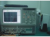
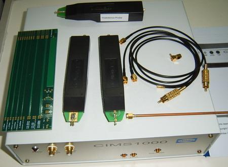
polar Impedance tester
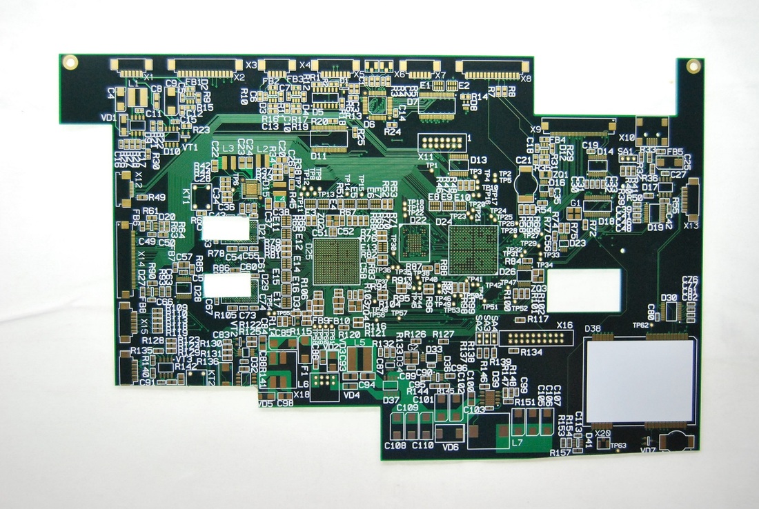
Our PCBs

Flex PCB
Rigid-flex PCB
RF board
Heavy copper PCB
20 layer PCB
10 layer PCB
HDI PCB
ENEPIG PCB
Control impadence
Quick Turn boards
MC PCB
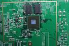
BGA Assembly
BGA assembly
Additional Products&Service

Components Sourcing
PCB Assemble
SMT Stencil
Cable assemble


About Us
Why Us
WorkShop
Quality
Testimonials
​Contact Us
Technology
Any layer HDI  PCB
Generate Gerber
Rigid-Flex Design Guide
10 Layer PCB
Impedance control
Heavy Copper PCB
​PCB Assembly
Quick Turn Circuits
HDI boards
Rigid-Flex circuits
RF/Microwave/HF PCB
MC PCB/Al-substrate
ENEPIG PCB
​Components procument


Payment
Shipment
FAQ
StormProto
SMT stencil
Via in Pad


Download
PCB Capability
Sample BOM
PCB check list
Multilayer stack up
​Stencils
PCB material

​
sales@stormcircuit.com​​             All rights reserved,2007-2020 Storm Circuit Technology Ltd
Picture
www.stormpcb.com
www.stormcircuit.com
Picture
Picture
Made with love by Storm Circuit in China

Picture
Picture
Picture

    news and discount

Subscribe
  • Home
  • PCB Fab
    • Standard PCB
    • ENEPIG PCB
    • HDI PCB
    • Impedance Control
    • Heavy Copper PCB
    • Via in Pad
    • Quick Turn PCB
    • 10 layer PCB
    • High frequency PCB
    • MC/Aluminum PCB
    • Half hole plating
    • FPC Rigid-flex PCB
    • StormProto PCB
  • Technology
    • PCB Terminology
    • PCB Material
    • PCB Stackup
    • Blind and burrid vias
    • Tip for PCB design
    • Generate gerber from Altium
    • Design guide for Flexible PCB
  • Blog
  • Product