Storm Circuit Blog
  • Home
  • PCB Fab
    • Standard PCB
    • ENEPIG PCB
    • HDI PCB
    • Impedance Control
    • Heavy Copper PCB
    • Via in Pad
    • Quick Turn PCB
    • 10 layer PCB
    • High frequency PCB
    • MC/Aluminum PCB
    • Half hole plating
    • FPC Rigid-flex PCB
    • StormProto PCB
  • Technology
    • PCB Terminology
    • PCB Material
    • PCB Stackup
    • Blind and burrid vias
    • Tip for PCB design
    • Generate gerber from Altium
    • Design guide for Flexible PCB
  • Blog
  • Product

Printed Circuit Boards Technology
​

Picture
Printed Circuit Board is a complex prodcut,it is one of the most widely used technological components today, used in everything from cell phones to smart home devices to military equipment. And when you work in the technology and development industry, you need access to the most advanced PCBs available.When we get a product, we may can not see the key technology,but it it there. like Apple phone,the main PCB in the cell phone has any layer HDI technology,that is a bit complex to do ,even some small headsets, it looks so small but why some headset only sell tens of USD,and some can sell with thousands of USD?

Download Full Capability
Contact us to get more details of PCB capability.
PCB Capability
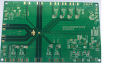
Storm Circuit offers a full range of PCB products,1-28 layers,flexible PCB,Rigid-flex circuit boards,HDI,high frequency PCB,RF circuit boards,microwave circuit boards. 
Layer count Production:1~28layers / Prototypes:30 Layers
Thickness Production:394mil(10mm)/ Prototypes:12mm
Material FR-4,High TG FR4,Halogen free,Ceramic filler,PTFE(Teflon), F4B,FPC Polymide,mix stack, (Arlon,Rogers,Taconic,,Nelco,Isola,Alu board,Copper board)
Trace/space 3/3 mil (0.076/0.076mm)
Copper weight 1-12oz
Hole Mechanical 6 mil (0.15mm) / Laser 3 mil (0.075mm)
Dimension 1230mm X 560mm (under 450*500 is preferred)
Finishing HASL ,HASL Lead Free, Immersion Gold, ENEPIG,Immersion Tin , OSP (Entek), HAL+Gold fingers,,Immersion Sivler
Special Burreid vias,blind vias,Countersunk holes,impedence control , burn-in board
About Us
Why Us
WorkShop
Quality
Testimonials
​Contact Us
Technology
Any layer HDI  PCB
Generate Gerber
Rigid-Flex Design Guide
10 Layer PCB
Impedance control
Heavy Copper PCB
​PCB Assembly
Quick Turn Circuits
HDI boards
Rigid-Flex circuits
RF/Microwave/HF PCB
MC PCB/Al-substrate
ENEPIG PCB
​Components procument


Payment
Shipment
FAQ
StormProto
SMT stencil
Via in Pad


Download
PCB Capability
Sample BOM
PCB check list
Multilayer stack up
​Stencils
PCB material

​
sales@stormcircuit.com​​             All rights reserved,2007-2020 Storm Circuit Technology Ltd
Picture
www.stormpcb.com
www.stormcircuit.com
Picture
Picture
Made with love by Storm Circuit in China

Picture
Picture
Picture

    news and discount

Subscribe
  • Home
  • PCB Fab
    • Standard PCB
    • ENEPIG PCB
    • HDI PCB
    • Impedance Control
    • Heavy Copper PCB
    • Via in Pad
    • Quick Turn PCB
    • 10 layer PCB
    • High frequency PCB
    • MC/Aluminum PCB
    • Half hole plating
    • FPC Rigid-flex PCB
    • StormProto PCB
  • Technology
    • PCB Terminology
    • PCB Material
    • PCB Stackup
    • Blind and burrid vias
    • Tip for PCB design
    • Generate gerber from Altium
    • Design guide for Flexible PCB
  • Blog
  • Product