Because of bad experience with weebly.We can not enable SSL for many years,but weebly can not fix this issue.Our latest news change to this link
https://www.stormpcb.com/PCBnews
https://www.stormpcb.com/PCBnews
|
4 layer RO4350B PCB with blind and ENEPIG designed by High Speed Intergated Circuits Lab. This PCB material is all Rogers 4350B 6.6mil, the stackup is as below. TOP Core RO4350B 6.6mil L2 PP RO4450F 8mil L3 Core RO4350B 6.6mil L4 Total thickness is 0.7mm The key technology is the pad size is the same as trace with only 4mil .and the PCB finish is ENEPIG ,and blind vias. Also,blind vias from L1-L2, L3-L4. min hole 0.15mm. 4mil trace /space and the pad size too at the main chip zone. Storm Circuit makes a lot of RF/High Frequency PCB with ENEPIG and Blind vias or buried vias ,from 2 layer to 12 layer RF PCB,high speed intergrated circuits .
0 Comments
This PCB was made with Rogers Material ,RO4003 0.508mm. 2 Layer, There are 9 different designs per panel . And full gold at top and bottom side for units in the panel . Plated slots .also,one slot requires only one side with plated, another side is unplated. This RF PCB looks very nice, it is very thin,only 0.6mm, full gold looks like transparent。 We know Amazon is the world's largest online retailer and a prominent cloud service provider. Many people buy goods from Amazon.
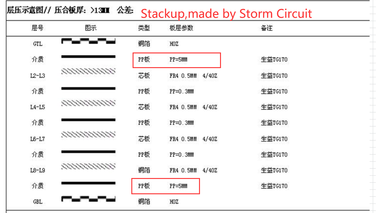
Headquartered in Seattle, Amazon has individual websites, software development centers, customer service centers, data centers and fulfillment centers around the world.Not only the sales on website ,Amazon has many software and hardware products. So,there are a lot of printed circuit boads they need too. We are so proud that we made some circuit boards for Amazon robitcs . This is a 6 layer PCB, with thickness 2.4mm, black solder mask. Immersion Gold. 1oz for all layers. Our client in American University has a new PCB design for charging pile.Everyone knows the main problem in charging pile is the high voltage,normal PCB will be broken down by high voltage. This PCB is very very thick, so far, this is the thickest we have made. it is about 13mm, 10 layer PCB and all inner layers are 4OZ, also,it has blind vias in inner layers. The thickness is the key technology and the dielectric thickness too. The PCB requires dielectric thickness between L1/L2 and L9/L10 is 5mm, 5mm dielectric thickness can pass 20KV. PCB stackup The key technology is the thickness, dielectric thickness is 5mm between L1/L2 and L9/L10. So, the total thickness will be about 13mm,including 4OZ for all inner layers thickness.  Storm Circuit can make PCBs from JPG . Some engineers only can use windows jpg software to draw trace/pads. They do not use professional PCB design software. So,we have to help customer to make PCBs from JPG ,generate gerber from jpg first. Here is an example shows how we help customers. We help our customer to win the prize category for the most ingenious machine. Because we finished the PCB in a very short time. 1 day to get gerber file from the jpg ,and 2 days to finish the PCB manufacturing. We are very proud to help our customers win important awards
12 LAYER PCB WITH ALL RO4350B WITH BLIND VIAS
Blind L1-L2,L1-L6 PCB thickness 2.6mm via in pad full gold at bottom side. Board dimension:272*280mm Lead time:12 days Storm Circuits made a lot of HDI PCBs this year. we have good capability now.
Here is an example for HDI 2+N+2 quick turn in 10 days. PCB Spec:FR4,TG170 .Shengyi S1000-2 material, Copper thickness 1OZ, min hole 0.1mm, min trace/space 0.1/0.1mm Blind/buried vias:L1-L2,L1-L3,L2-L3,L3-L6,L6-L7,L7-L8 finish the PCB in 10 days. Rogers material + FR4 high TG with blind vias PCB Stackup. Storm Circuit can make such hybrid stackup PCB. This is a 6 layer PCB ,Blind vias from L1-l2. Below is the 3D image to show the control depth slot.
PCB spec: Material:Rogers material RO4350B+FR4 (TG170) Board thickness:1.45mm Blind via:L1-L2 Min trace:0.1mm Min space:0.1mm Surface finish:Immersion Gold Impedance control, Many PCB assembly factories do not make prototypes, they only want to do production, like 1K,10k pcs. however, we can offer any QTY to do ,prototypes are first. Below is an example of the PCB assembly prototypes. there are 115 items components and min chip is 0402,both SMT side .we offered full turnkey assembly service, including PCB fabrication ,components sourcing and assembly.
|
|
sales@stormcircuit.com All rights reserved,2007-2020 Storm Circuit Technology Ltd
|
|