How to test a PCB by fly probe
Many customers asked us what are the difference for fly probe testing and fixture (jig) testing? Here,we show you how to test a PCB by fly probe. Fly probe testing is mostly for prototypes as it costs much time.However,a fixtures or jig is for production QTY to test.it is very quick,1-2 seconds per panel . Fly probe testing is one by one point,if test points are many,at least 10 mins per panel.so 1 hour only can test 6 or so panels. that is difference.
Anyway,if you have production QTY in the future,so we would like you to do with fixture to test,and prototypes only for fly probe. Fly probe cost is lower but each time,we have to charge ,for fixture cost,we only charge the first cost.free for next repeat order.
Anyway,if you have production QTY in the future,so we would like you to do with fixture to test,and prototypes only for fly probe. Fly probe cost is lower but each time,we have to charge ,for fixture cost,we only charge the first cost.free for next repeat order.
|
More vedios ,follow our youtube.
|
|
PCB Manufacturing Process
PCB (Printed Circuit Boards) is a complex process ,any mistakes in the process will damage the boards.There are many types of Printed Circuit Boards,we will show you a simple PCB making here.
- Single-sided circuit boards----just one copper layer and usually the copper is at bottom layer. the holes are also usually non-plated.
- Double-sided circuit boards---two copper layer-top and bottom layers. the holes have to be plated to be conducted
- Multi-layer circuit boards----more than 2 copper layers.there are some inner layers with copper to press with top/bottom. Multi-layers are usually even numbers. Four layers circuit boards have to use one core material and press with two copper foil . Six layers circuit boards have to use two cores material,eight layers circuit boards have to use three core material.
|
|
A simple PCB process flowMaterial/Tooling Preparation (CAM engineering)-->Photo plotter (Film)--->Inner layer (UV Expose,Etching,Striping)--->Lamination (lay up,Pressing)--->Drilling--->PTH (Panel plating)--->Outer layer(UV expose,etching,striping)--->solder mask(expose)---〉Silkscreen(legend printing)--->Surface finishing--->FQC--->Packing
Note:Each process,QC/QA will inspect all boards 8 layer stack up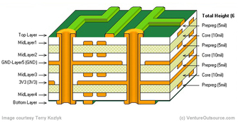
|